Defect-Tolerant Nanophotonic Film
I designed a computational nanophotonics study around a simple question: can an optical metasurface remain useful after realistic fabrication defects are introduced? The model is a 6 × 6 periodic supercell of TiO₂ nanodisks on glass, with missing disks, radius and height variation, and positional jitter. Instead of optimising only a perfect geometry, I designed the Tidy3D FDTD workflow around robustness — transmission, reflection, diffraction, field behaviour, and a quantitative defect-sensitivity metric. I also iterated through earlier Tidy3D models and completed multiple solver runs. Those development runs used earlier geometry and wavelength settings, so I treat them as evidence of the simulation workflow rather than validation of the final visible-band defect-tolerance study.
Summary
- Physics & Modeling
- Major project
- In development
Evidence on file
My contribution
I wrote the research question and hypothesis, specified the metasurface geometry and the 6 × 6 supercell, chose the TiO₂, glass and air material model, defined the eight defect cases, exported the simulation geometry, and laid out the Tidy3D setup — source, boundaries, mesh and the five monitors. I also defined the analysis metrics including the Defect Sensitivity Index, wrote the parameter-sweep plan and the numerical validation checklist, and planned how the results would be presented.
I ran earlier FDTD iterations while developing the project, including saved flux and field-monitor results. The later 450–750 nm TiO₂ defect matrix documented here was designed afterward and was not rerun, so the earlier results are shown separately rather than treated as validation of the final study.
Project overview
Why I built this
Can a subwavelength nanophotonic film maintain high visible transmission and low haze after realistic fabrication defects are introduced?
The hypothesis is that broad, low-Q all-dielectric behaviour should be less fragile than a narrowly resonant design. If the period stays below the visible diffraction threshold in the substrate, and the disks are not tuned to a sharp resonance, then moderate radius errors, small positional jitter and even a few missing disks should perturb broadband transmission only weakly.
That is a hypothesis. Testing it is what the simulation matrix is for.
Why defect tolerance matters
A perfect periodic structure can produce striking optical effects. Real fabricated films contain imperfections — lithography varies the radius, etching varies the depth, pattern transfer shifts positions, and particles or mask failures remove features entirely.
So there are two versions of this project. One asks whether an optical effect can be produced at all, tunes for maximum resonance, and shows a field plot. The other asks whether the design still works when reality is imperfect, compares pristine against defective supercells statistically, and trades optical performance against manufacturability.
The second is the one worth building, and it changes what counts as a good design. A sharp high-Q resonance gives the strongest nominal performance and is destroyed by the errors a real process introduces. A broad low-Q response gives less on paper and may survive.
The intended application sets the same priority. A light-management coating for a display cover, architectural glass, a solar window or an optical sensor needs high transmission and low haze far more than it needs an extremely narrow spectral feature.
Device concept
An all-dielectric TiO₂ nanodisk array on a glass substrate, illuminated from air. The starting values come from the research plan, and each is a choice with a reason rather than a tuned optimum.
- 0.28 µm — below the wavelength in glass across most of the visible band, which keeps diffraction and haze down.
- 0.07 µm — moderate fill fraction, avoiding an excessively strong or narrow resonance.
- 0.22 µm — enough for phase and scattering control while staying fabricable.
- 6 × 6 cells, 1.68 µm square — large enough to carry defect patterns, small enough to simulate.
- TiO₂, n ≈ 2.35 assumed — high index, low loss in the visible.
- Glass / SiO₂, n ≈ 1.45 assumed.
- Air, n = 1.00.
- Both indices are simplified nondispersive approximations, not material measurements. A final version would import wavelength-dependent optical constants.
Interactive 3D model
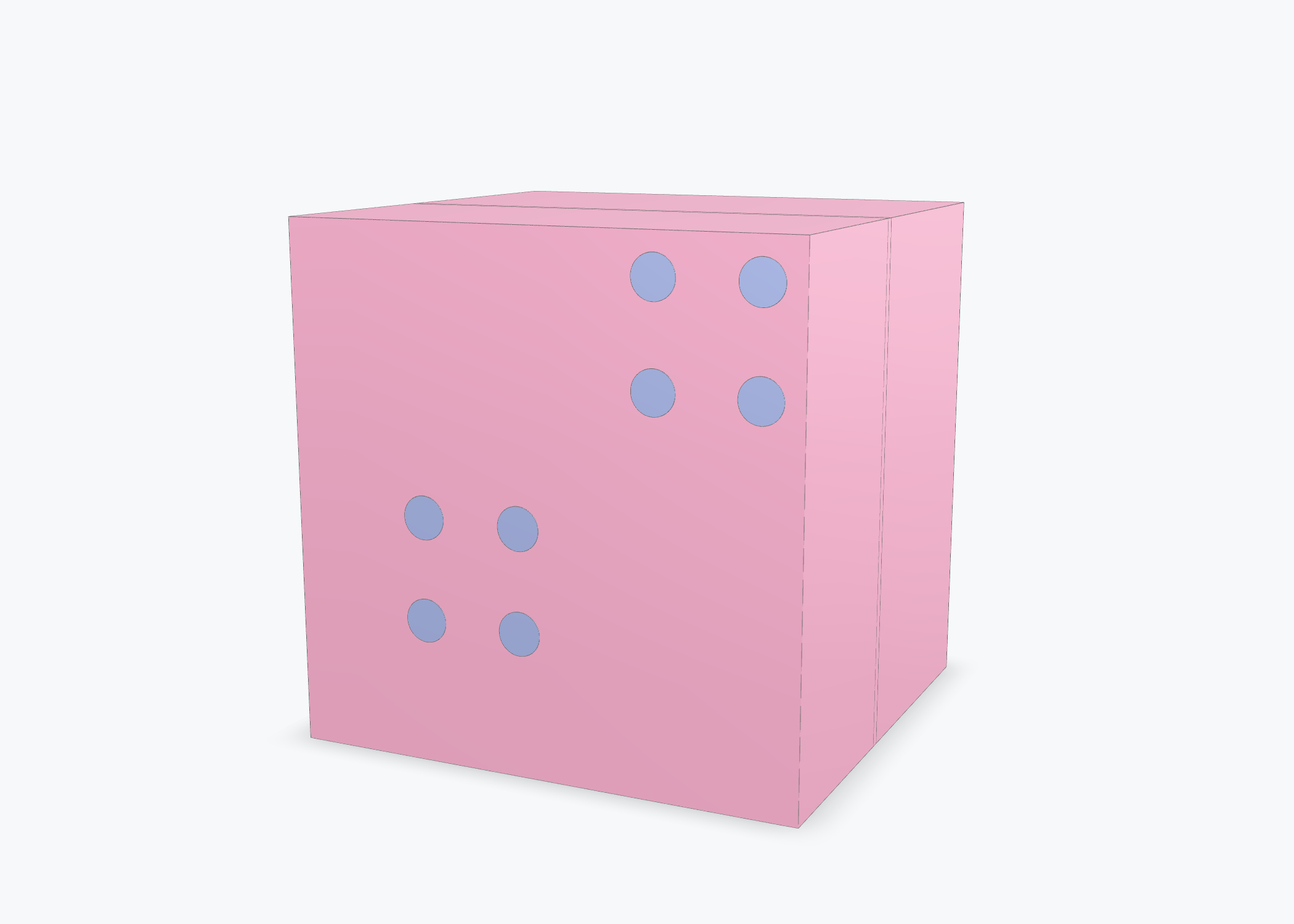
The Tidy3D scene as currently exported, turnable in the browser. The pink volume is the simulation domain with the substrate inside it, and the blue cylinders are nanodisks.
Two things about this export are worth stating plainly. It is the scene as it stands rather than the finished specification: the domain footprint is 1.34 µm and it holds a handful of disk positions, not the 1.68 µm 6 × 6 array at R = 0.07 µm that the geometry table and the defect map describe. And the domain boundary is opaque from most angles, so much of what sits inside is hidden. Building the full supercell in Tidy3D is part of what is still ahead.
Loading the interactive model…
Simulation geometry only. Nothing here has been fabricated, and no simulation has been run on it.
Simulation geometry exports
Earlier FDTD development runs
Before the visible-band study was written, the project went through nine Tidy3D revisions, V1 to V9, all of which completed successfully. V9 is the one whose data survived. It is a genuine solver result belonging to an earlier model iteration, not to the study described on this page.
The differences matter. Its flux monitors sweep approximately 1.50 to 1.60 µm — telecom, not the 450 to 750 nm visible range the final study is built around — and its geometry and materials differ from the final TiO₂ supercell. So these are development evidence: the workflow ran end to end and produced real monitor data. They do not test the defect-tolerance hypothesis.
The flux values are raw directional monitor flux, not normalised reflectance or transmittance; turning them into percentages needs an incident-power normalisation nobody has documented. The sign follows the monitor surface-normal / flux-direction convention; it does not represent negative optical power.
Earlier Tidy3D development history. Versions V1 through V9 completed successfully; V10 remained a draft. Successful earlier runs are evidence of the simulation-development process, not validation of the later visible-band TiO₂ defect study.
Tidy3D Results workspace for the successful V9 development model, showing saved reflection, transmission and field-monitor datasets. V9 used an earlier model configuration and is not the final 450–750 nm defect-tolerance study.
EARLIER FDTD DEVELOPMENT RESULT — V9. Raw directional flux from the V9 reflection monitor, 1.50–1.60 µm. The sign follows the monitor surface-normal convention; it does not represent negative optical power.
EARLIER FDTD DEVELOPMENT RESULT — V9. Raw directional flux from the V9 transmission monitor, 1.50–1.60 µm. Not a transmittance percentage.
Earlier FDTD development result — V9. Vertical |E|² from the stored field monitor at approximately 580 nm. This belongs to the earlier V9 model, not the final 6 × 6 TiO₂ defect geometry. The field monitors store discrete wavelengths and are separate from the 1.50–1.60 µm flux sweep.
Earlier FDTD development result — V9. Surface |E|² from the stored field monitor at approximately 620 nm. This belongs to the earlier V9 model, not the final 6 × 6 TiO₂ defect geometry. The field monitors store discrete wavelengths and are separate from the 1.50–1.60 µm flux sweep.
The 6 × 6 supercell
6 × 6 TiO₂ nanodisk supercell used to define a defective geometry. Highlighted cells mark intentionally missing disks; remaining disks can also include size or position perturbations.
This is a geometry and defect-layout figure, not a simulation result. It shows the arrangement the study is built around — period 0.28 µm, nominal radius 0.07 µm, and the 1.68 µm square that repeats periodically in x and y.
Defects built into the study
Eight cases, each compared against the pristine film using the same source, monitors, mesh and wavelength sampling. These eight final defect cases were defined after the earlier solver iterations. The final D0–D7 matrix was not run.
| Case | Defect | Value | What it tests |
|---|---|---|---|
| D0 | Pristine | No defects | Baseline performance. |
| D1 | Radius variation | σR = 5 nm | Mild lithography or etch-radius variation. |
| D2 | Radius variation | σR = 10 nm | Moderate fabrication error. |
| D3 | Height variation | σH = 10 nm | Etch-depth nonuniformity. |
| D4 | Positional jitter | σx,y = 10 nm | Placement or pattern-transfer error. |
| D5 | Missing nanodisks | 5 % removed at random | Particle, mask or processing failures. |
| D6 | Missing nanodisks | 10 % removed at random | Severe but plausible defect-tolerance test. |
| D7 | Combined disorder | σR = 10 nm, σx,y = 10 nm, 5 % missing | More realistic combined-disorder test. |
Simulation architecture
The Tidy3D setup, from illumination to recorded data. Values are the specification rather than a tuned configuration.
- 01
Plane-wave source, 450–750 nm
Propagating in −z from air into the film, Ex polarisation first and Ey repeated. Centre wavelength 550 nm for field snapshots.
- 02
Periodic x/y boundaries
Models an infinite repeated film. Bloch boundaries for the 15° and 30° angled-incidence checks.
- 03
PML z boundaries
Absorbs outgoing reflected and transmitted waves so nothing re-enters the domain.
- 04
Reflection flux monitor
Above the source and below the top PML. Gives R(λ).
- 05
Transmission flux monitor
Below the substrate and above the bottom PML. Gives T(λ).
- 06
Diffraction monitor
On the transmission side. Power in the allowed nonzero orders — the haze proxy.
- 07
Field monitors, xz and xy
A vertical slice through the disks and a horizontal plane at disk mid-height, at 550 nm.
- 08
Field-time monitor (optional)
One point below the film, to confirm the fields have decayed before the run stops.
How I would measure robustness
The point of the study is to turn field pictures into numbers. Five quantities come out of the monitor data, and each answers a different question.
- T(λ), transmitted power over incident power, across 450 to 750 nm. Whether the film stays optically useful.
- R(λ), reflected power over incident power. Whether the film manages light rather than merely scattering it.
- A = 1 − T − R should sit near zero for lossless approximations. A deviation is a numerical warning, not material absorption.
- Transmitted power in nonzero diffraction orders over total transmitted power. Whether the film would look clear or cloudy.
- The mean over wavelength of |T_defect(λ) − T_pristine(λ)|, divided by the mean pristine transmission. A smaller DSI means a less sensitive film.
- It replaces a judgement about whether two curves look similar with one figure that can be compared across defect cases and reported with a spread.
Numerical validation
A simulation result that has not been checked against its own numerics is a picture, not evidence. These checks were defined for the final visible-band defect study and were not completed for that revised model.
Mesh convergence: repeat the best design at 20, 25 and 30 steps per wavelength; the curves should move only slightly. If they move a lot, the mesh is the result.
Domain convergence: increase the air and substrate buffers and confirm T and R do not shift, which tests whether the absorbing boundaries sit too close.
Energy conservation: confirm T + R + numerical loss stays close to one for the lossless approximation.
Defect randomness: repeat the 5 per cent and 10 per cent missing-disk cases with at least three random seeds and report mean and spread, because one seed is one arrangement, not a statistic.
Polarisation: repeat with Ex and Ey at normal incidence. A large difference implies anisotropy in the geometry or the defect arrangement.
Incidence angle: test 15 and 30 degrees with Bloch boundaries, since a coating on a window is not used at normal incidence only.
What would count as a convincing result
Four acceptance criteria, set in advance so the study can fail. Every value below is a design target that has not been measured — the simulations that would produce these numbers have not been run.
| Status | Criterion | Target | Why it matters |
|---|---|---|---|
| TARGET — NOT YET MEASURED | Average transmission, 450–750 nm | > 85 % after 10 % missing-disk defects | Shows the film remains optically useful. |
| TARGET — NOT YET MEASURED | Average reflection | < 8 % across most of the visible band | Demonstrates light management, not just scattering. |
| TARGET — NOT YET MEASURED | Haze proxy | < 3 % pristine, < 5 % for the 10 % defect case | Makes the film plausible for display or window use. |
| TARGET — NOT YET MEASURED | Defect Sensitivity Index | < 0.06 for 10 % defects | Quantifies robustness rather than relying on appearance. |
Current state and what is still pending
What was completed: nine Tidy3D development revisions were set up and successfully solved. The surviving V9 dataset holds real solver output — four flux monitors across 1.50 to 1.60 µm and two field monitors at five wavelengths each — and those files are on this page.
What remained unfinished: the final 450 to 750 nm 6 × 6 TiO₂ defect-tolerance study was not rerun after the revision. Still uncompleted for that model are the pristine baseline, the D0–D7 matrix, its field maps, normalised transmission and reflection spectra, the diffraction and haze analysis, the parameter sweeps, the convergence tests, the repeated seeds, and the robustness statistics and Defect Sensitivity Index that depend on all of it.
The design and geometry do exist — question, specification, defect supercell, exported scene, monitor plan, metrics and validation checklist — and the export still has to catch up with the specification.
This page will change when the final results exist. Until then it separates what was solved from what was designed.
What I learned
I started out thinking a good nanophotonic design meant optimising the perfect geometry — find the radius and height that maximise the effect, render the field map, done.
The stronger engineering question turned out to be whether the design remains useful when fabrication is imperfect. That changed what I was optimising. Instead of best nominal performance, the target became performance plus robustness plus validation, and the three are in tension: the sharpest resonance is usually the most fragile one.
It also changed what counts as evidence. A field map is the most attractive output a solver produces and the least informative: it shows one wavelength, one geometry, one moment. Robustness needs spectra across the band, the same defect case repeated with different random seeds, convergence checks proving the mesh is not the answer, and a number with a spread attached rather than two curves that look close.
The earlier runs taught me another distinction: a solver returning Success is not the same as answering the final research question. The visible-band study changed the geometry, wavelength range, defect matrix and validation criteria enough that I could not honestly use the earlier results as proof of the final hypothesis. Keeping those two things apart is scope control, and it is cheaper to do while writing the page than after someone asks.
Evidence
Related work
I built and simulated a crossed-nanowire optical detector model in Tidy3D FDTD, using orthogonal NbTiN detector elements inside a multilayer SiO₂ and gold optical stack. The completed V1 run records electric-field distributions and directional flux near 1.55 µm. The crossed geometry was intended to reduce polarization dependence, but the surviving simulation uses only one incident linear polarization — so polarization insensitivity remains a design goal rather than a demonstrated result.
I developed a multi-element broadband optical-delivery model in Ansys Zemax OpticStudio and evaluated it across multiple wavelengths, field angles, and three saved configurations. The prescription uses fused silica and CaF₂ elements with multiple powered and AR-coated surfaces. Native analyses include configuration-matrix spot diagrams, polychromatic diffraction encircled energy, and wavefront evaluation. The design concept included polarization preservation as an objective, but the saved evidence here does not contain a polarization-specific metric, so I do not present that behavior as demonstrated.
I developed two related sequential optical models in Ansys Zemax OpticStudio to study how a microlens could direct broadband solar illumination toward a small rectenna microcell plane. The models explore different lenslet geometries, wavelength ranges, and field angles. Native OpticStudio outputs include 3D layout, optical-path-difference analysis, and saved 850-nm wavefront results. Because the two prescriptions and pupil conditions differ, I treat their results as evidence of design exploration rather than a controlled before-and-after performance comparison.